[논문/Matter] Layer-engineered atomic-scale spalling of 2D van der Waals crystals
작성자
관리자작성일자
2022-11-16 10:17조회수
69KIURI 박형기 참여연구원 논문
Matter. 2022 Aug 15; doi: 10.1016/j.matt.2022.07.021
Layer-engineered atomic-scale spalling of 2D van der Waals crystals
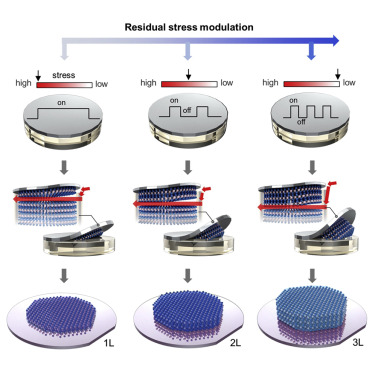
Transition-metal dichalcogenides (TMDCs), whose physical properties can be modified by the number of layers within the atomic thickness range, are emerging as an essential active interlayer for nanoelectronic devices based on van der Waals (vdW) heterostructures. Here, we show the atomic spalling of vdW crystals that achieves large-area TMDCs with a controlled number of layers. Unlike 3D covalent network solids, the TMDCs are layered crystals featuring strong in-plane covalent bonding and weak out-of-plane vdW interaction, which allow the crack propagation depth to be reduced to the atomic scale. By adjusting the residual stress of the stressor film, we controlled the crack propagation depth at a scale corresponding to the monolayer thickness of the TMDCs. Consequently, mono-, bi-, and trilayer TMDCs were selectively separated from the vdW crystals. The presented results show huge potential for the manufacture of layer-engineered, high-quality vdW materials, which can be developed into functional optoelectronic devices.
